GALLIUM NITRIDE (GaN) WAFERS
Unleashing High-Power Innovation
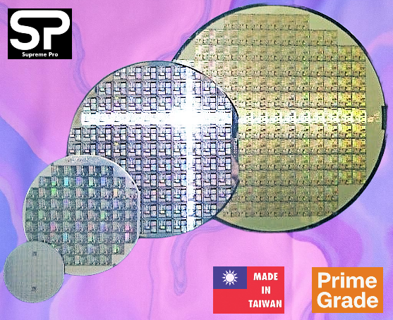
Image shown is a representation only. Exact specifications should be obtained from the product data sheet.Gallium Nitride (GaN) wafers are pivotal in power electronics and RF applications, driven by demand in electric vehicles (EVs), 5G telecommunications, and data centers. Classified as a compound semiconductor, our GaN wafers are at the forefront of next-generation power and RF electronics, delivering unparalleled efficiency and performance. Engineered through our Singapore-Taiwan partnership, leveraging Taiwan’s 60% global semiconductor dominance, our GaN-on-Si and GaN-on-SiC wafers offer high electron mobility, wide band gap, and superior thermal conductivity. Designed for automotive-grade reliability, they enable compact, energy-efficient solutions for EVs, 5G infrastructure, and data centers. Partner with us to power your high-frequency, high-voltage applications with cutting-edge technology.
Our GaN Wafers
2-inch GaN-on-Si Epitaxial Wafer
2-inch GaN Template Wafer on Sapphire
4-inch (100mm) GaN-on-Si Epitaxial Wafer
4-inch (100mm) GaN-on-SiC Epitaxial Wafer
6-inch (150mm) GaN-on-Si Epitaxial Wafer
6-inch (150mm) GaN-on-SiC Epitaxial Wafer
8-inch (200mm) GaN-on-Si Epitaxial Wafer
8-inch (200mm) GaN Template Wafer on SiC
+ We offer fully customizable GaN wafers and substrates to suit your unique needs, including specialized epitaxial options. Contact us today for a personalized quote and explore how our tailored solutions can elevate your projects.
WHY CHOOSE GaN WAFERS?
High Performance
GaN’s wide band gap and high electron mobility enable 100x faster switching, ideal for 5G and EV markets.
Cost Efficiency
Scalable 300mm wafers reduce production costs by 2.3x compared to 200mm, nearing silicon cost parity.
Reliability
Low dislocation density (≤10⁸/cm²) and AEC-Q100 compliance ensure consistent performance in critical applications.
Compact Solutions
High power density supports 50% smaller devices, meeting demand for lightweight EV and consumer electronics.
Future-Proof
Aligned with the $20.11 billion GaN market’s 22.7% CAGR, our wafers drive innovation in AI, 5G, and renewables.
WHY CHOOSE US?


Superior Quality
Leveraging Taiwan’s 60% global chip share, we deliver Prime Grade 4H-GaN wafers with dislocation density ≤10⁸/cm², meeting stringent AEC-Q100 standards for automotive and aerospace applications.
Cost Efficiency
Our focus on yield optimization (up to 85% in 2026 scenarios) and reusable wafer technologies reduces costs by up to 30%, addressing buyer concerns about GaN’s high cost vs. silicon.
Custom Solutions
We offer tailored wafer specifications (e.g., doping, thickness) and dedicated support, matching key player’s customer-centric approach, to meet unique project needs.
Sustainability Focus
Our GaN wafers enable energy-efficient devices, reducing EV ownership costs by ~$4,000 and supporting decarbonization, aligning with buyer priorities for green technology.


Advanced Manufacturing
Partnering with Taiwanese leaders in this sector, we use cutting-edge PVT and CVD processes to ensure low-defect, high-uniformity wafers, scalable to 200mm for cost-efficient production.
Reliable Supply Chain
Unlike competitors facing 20% supply shortages, our vertically integrated supply chain, inspired by STMicroelectronics’ Catania campus, ensures consistent delivery and extended longevity programs.
Global Trust
Certified to ISO 9001, ISO 14001, RoHS, and REACH standards, our wafers are trusted by OEMs in 45+ countries, backed by Singapore-Taiwan expertise.
Ready to elevate your designs with our GaN Wafers? Click below to request a quote or discuss custom specifications.
SPECIFICATIONS
Material: GaN-on-Si (primary), GaN-on-SiC, GaN-on-Sapphire (custom options)
Diameter: 100mm, 150mm, 200mm (scalable for high-volume production)
Thickness: 400–650 µm (customizable per application)
Dislocation Density: ≤10⁸/cm² (low-defect for high reliability)
Surface Finish: Metal Organic Chemical Vapor Deposition (MOCVD), mirror-like, Ra <0.5 nm
Doping: N-type (Si-doped) or P-type (Mg-doped) for power and RF applications
Thermal Conductivity: 130–200 W/m·K (GaN-on-SiC), 50–70 W/m·K (GaN-on-Si)
Breakdown Electric Field: 3.3 MV/cm (10x silicon)
Bandgap: 3.4 eV (3x silicon for high-temperature operation)
Electron Mobility: 1,500–2,000 cm²/V·s (2x silicon for faster switching)
Crystal Structure: Wurtzite, optimized for HEMTs and power devices
Packaging: Class 100 cleanroom, vacuum-sealed for contamination-free delivery
Contact Us: Inquire about custom specifications or pricing. Click below to connect with our team.
STANDOUT FEATURES


Superior Thermal Conductivity
130–200 W/m·K (GaN-on-SiC) dissipates heat efficiently, enhancing device lifespan in high-power systems.
Wide Band Gap
3.4 eV supports high-voltage operation (up to 600V), reducing cooling needs for compact designs.
Lower Capacitance
Up to 90% reduced parasitic capacitance (8-inch wafers) enhances high-frequency performance.
Advanced Surface Quality
CMP delivers a mirror-like finish (Ra <0.5 nm), ensuring optimal epitaxial layer growth for high-performance devices.
Scalable Wafer Sizes
100mm to 300mm diameters, with 300mm offering 2.3x more chips per wafer, reducing costs.

High Electron Mobility
1,500–2,000 cm²/V·s enables ultra-fast switching, ideal for 5G RF amplifiers and EV chargers.
High Breakdown Field
3.3 MV/cm (10x silicon) ensures robust performance in high-voltage EV and 5G applications.
Low Dislocation Density
≤10⁸/cm² ensures high reliability and yield, critical for automotive and defense applications.
ADDITIONAL BENEFITS

Enhanced Efficiency
Up to 40% energy savings in power supplies, reducing operating costs in data centers and EVs.

Thermal Resilience
Operates at temperatures up to 400°C, ensuring reliability in aerospace and industrial applications.
Compact Designs
High power density enables 50% smaller chargers and inverters, cutting EV production costs by ~$1,500 per vehicle.
Contact Us: Discover how our GaN wafers can optimize your designs. Click below for a quote.
High-Frequency Performance
100x faster switching speeds support 5G base stations and radar systems, improving signal reliability.


Sustainability
GaN’s efficiency reduces carbon emissions by 10x compared to silicon, supporting green initiatives.
INDUSTRIES, APPLICATIONS & SYSTEMS USING GaN WAFERS


Power Electronics
GaN HEMTs (High Electron Mobility Transistors)
GaN Power Switches / High-Efficiency Switches
GaN Inverters & Power Converters
GaN Power Modules
GaN High-Voltage Transistors & Switches
GaN Power Management Units (PMUs)
GaN High-Power Rectifiers
GaN High-Voltage Power Supplies
Electric Vehicle (EV) Powertrains
On-Board Chargers (OBC)
Battery Management Systems (BMS)
Vehicle-to-Everything (V2X) Communication Modules
Aircraft Radar Systems (Airborne AESA Radars)
Spacecraft Power Management Units (PMUs)
Space Exploration Electronics (Deep-Space Communication, Power Systems)
Satellite Communication Payloads
Satellite Broadband Networks
Radar Systems (Ground, Naval & Airborne)
Military Communication Systems
Missile Defense Radar & Guidance Systems
5G Base Stations (RF Power Amplifiers, Small Cells)

Industries
Electric Vehicles
Aerospace
Defense
Telecommunications
Data Centers
Renewable Energy
Sensors & Harsh-Environment Devices
GaN High-Temperature Transistors / Components
GaN High-Temperature Sensors
GaN Corrosion-Resistant Sensors
GaN Radiation-Hardened / Radiation-Resistant Devices
GaN High-Frequency Sensors


Systems / Devices
Power Grids
Industrial & Automation
Consumer Electronics
Medical
Research & Development

Applications
RF & Microwave Devices
GaN RF Transistors
GaN Power Amplifiers
GaN RF Modules
GaN High-Frequency Amplifiers / Oscillators
GaN High-Power Microwave Devices
GaN Electronic Warfare Components
GaN High-Frequency Devices & Test Structures


Optoelectronics
GaN LEDs (Light-Emitting Diodes)
GaN Optoelectronic Components

Wireless Communication Infrastructure (Microwave & mmWave Systems)
Data Center Servers (Power Supplies, Cooling Subsystems)
High-Speed Computing Systems (AI Accelerators, HPC Servers)
Solar Inverters
Wind Turbine Power Conversion Systems
Energy Storage Unit (ESS) Converters
Smart Grid Infrastructure
Renewable Energy Integration Systems
Power Distribution Networks
Industrial Motor Drives
Factory Automation Systems
Robotics Power Electronics

At Supreme Pro, we offer fully customizable GaN wafers and substrates to suit your unique needs, including specialized epitaxial options. Contact us today for a personalized quote and explore how our tailored solutions can elevate your projects.
Research Applications
GaN Quantum Electronics Substrates
GaN Experimental Devices
Heavy-Duty Industrial Equipment
Mining Machinery
Offshore Platform Electronics (Oil & Gas)
Downhole Monitoring Systems
Chemical Reactor Power Systems
Process Control Units
Smartphones (Fast Charging Circuits, RF Front-End Modules)
Medical Imaging Devices (Ultrasound, CT, MRI Power Systems)
Portable Diagnostic Equipment
Radiation Therapy Machines
University Laboratory Systems
Innovation Centers
Technology R&D Facilities
Our GaN Wafers
2-inch GaN-on-Si Epitaxial Wafer
2-inch GaN Template Wafer on Sapphire
4-inch (100mm) GaN-on-Si Epitaxial Wafer
4-inch (100mm) GaN-on-SiC Epitaxial Wafer
6-inch (150mm) GaN-on-Si Epitaxial Wafer
6-inch (150mm) GaN-on-SiC Epitaxial Wafer
8-inch (200mm) GaN-on-Si Epitaxial Wafer
8-inch (200mm) GaN Template Wafer on SiC