SILICON CARBIDE (SiC) WAFERS
Powering the Future of Electronics


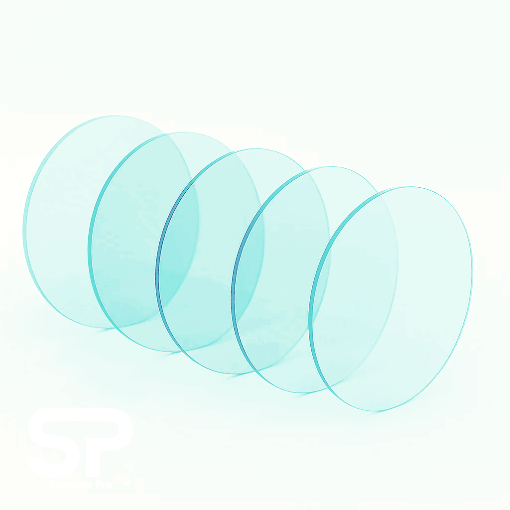
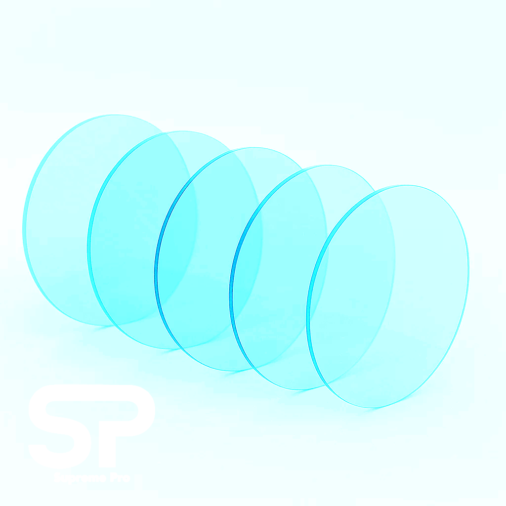
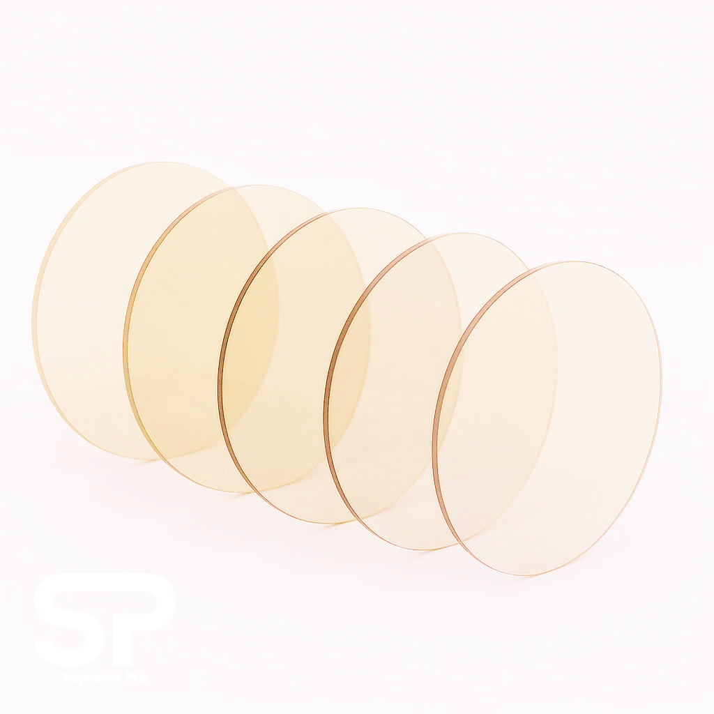

Image shown is a representation only. Exact specifications should be obtained from the product data sheet.Silicon Carbide (SiC) wafers are critical for high-performance power electronics, driven by demand in electric vehicles (EVs), renewable energy, and 5G telecommunications. Classified as a compound semiconductor, our SiC wafers are engineered to redefine performance in high-power, high-frequency, and high-temperature applications. Sourced from Taiwan’s world-leading semiconductor ecosystem and leveraging Singapore’s status as a global business hub, our SiC wafers deliver unmatched thermal conductivity, high-voltage resilience, and superior electron mobility.
Designed for automotive-grade reliability, our wafers enable compact, efficient, and sustainable solutions for electric vehicles, renewable energy, 5G systems, defense and aerospace. Backed by world-class quality and cost-effective pricing, these wafers are your gateway to cutting-edge innovation and efficiency in your next-generation devices.
Our SiC Wafers
4 inch Silicon Carbide Wafers 4H-SiC N-Type or Semi-Insulating SiC Substrates
4 inch High Purity (Undoped) Silicon Carbide Wafers Semi-Insulating SiC Substrates (HPSI)
6 inch Silicon Carbide Wafers 4H-SiC N-Type or Semi-Insulating SiC Substrates
6 inch High Purity (Undoped) Silicon Carbide Wafers Semi-Insulating SiC Substrates (HPSI)
8 inch Silicon Carbide Wafers 4H-SiC N-Type or Semi-Insulating SiC Substrates
8 inch High Purity (Undoped) Silicon Carbide Wafers Semi-Insulating SiC Substrates (HPSI)
+ We offer fully customizable SiC wafers and substrates to suit your unique needs, including specialized epitaxial options. Contact us today for a personalized quote and explore how our tailored solutions can elevate your projects.
WHY CHOOSE SiC WAFERS?
Unmatched Performance
SiC’s wide bandgap and high thermal conductivity enable smaller, lighter, and more efficient devices, critical for EV and 5G markets.
Scalability
Transition to 200mm wafers increases chip yield by up to 30%, reducing costs and meeting high-volume demand.
Reliability
Low defect density (MPD ≤5/cm²) and AEC-Q100 compliance ensure consistent performance in mission-critical applications.
Sustainability
High-efficiency SiC devices reduce energy consumption, supporting decarbonization goals (78% CO2 reduction in EVs).
Future-Proof
Aligned with the $2.65 billion SiC market’s 22.24% CAGR, our wafers drive innovation in AI, 5G, and renewable energy.
WHY CHOOSE US?


Superior Quality
Leveraging Taiwan’s 60% global chip share, we deliver Prime Grade 4H-SiC wafers with micropipe density ≤5/cm², meeting stringent AEC-Q100 standards for automotive and aerospace applications.
Cost Efficiency
Our focus on yield optimization (up to 90% in 2026 scenarios) and reusable wafer technologies reduces costs by up to 30%, addressing buyer concerns about SiC’s high cost vs. silicon.
Custom Solutions
We offer tailored wafer specifications (e.g., doping, thickness) and dedicated support, matching key player’s customer-centric approach, to meet unique project needs.
Sustainability Focus
Our SiC wafers enable energy-efficient devices, reducing EV ownership costs by ~$2,000 and supporting decarbonization, aligning with buyer priorities for green technology.


Advanced Manufacturing
Partnering with Taiwanese leaders in this sector, we use cutting-edge PVT and CVD processes to ensure low-defect, high-uniformity wafers, scalable to 200mm for cost-efficient production.
Reliable Supply Chain
Unlike competitors facing 20% supply shortages, our vertically integrated supply chain, inspired by STMicroelectronics’ Catania campus, ensures consistent delivery and extended longevity programs.
Global Trust
Certified to ISO 9001, ISO 14001, RoHS, and REACH standards, our wafers are trusted by OEMs in 45+ countries, backed by Singapore-Taiwan expertise.
Contact Us: Ready to elevate your designs with our SiC Wafers? Click below to request a quote or discuss custom specifications.
SPECIFICATIONS
Material: 4H-SiC (primary polytype for power electronics; 6H-SiC for specific RF applications)
Diameter: 100mm, 150mm, 200mm (8-inch gaining traction for high-volume cost efficiency)
Thickness: 350–500 µm (customizable, with ±25 µm tolerance for standard grades)
Micropipe Density (MPD): ≤1/cm² (Ultra-Prime Grade) or ≤5/cm² (Prime Grade) for low-defect performance
Resistivity Uniformity: ≥95% (ensuring consistent doping across the wafer)
Surface Finish: Chemical Mechanical Polishing (CMP), epi-ready, Ra <0.2 nm for optimal epitaxial growth
Doping: N-type (nitrogen-doped, resistivity 0.015–0.028 Ω·cm) or semi-insulating (vanadium-doped, >10^5 Ω·cm)
Thermal Conductivity: 370–490 W/m·K (superior heat dissipation, 3x silicon)
Breakdown Electric Field: 2.5–3.5 MV/cm (10x silicon for high-voltage resilience)
Bandgap: 3.26 eV (wide bandgap enabling 3x silicon's temperature tolerance)
Crystal Orientation: (0001) with 4° off-axis (optimized for epitaxial layer quality in power devices)
Total Thickness Variation (TTV): <5 µm (for uniform processing)
Bow/Warp: <25 µm bow, <40 µm warp (minimizing handling issues)
Packaging: Class 100 cleanroom, vacuum-sealed in anti-static containers for contamination-free transport
Contact Us: Inquire about custom specifications or pricing. Click below to connect with our team.
STANDOUT FEATURES


High Thermal Conductivity
370–490 W/m·K ensures efficient heat dissipation, ideal for high-power EV inverters and 5G amplifiers.
Wide Band Gap
SiC’s 3.26 eV band gap (vs. silicon’s 1.12 eV) supports higher voltages and temperatures, reducing cooling needs.
Chemical Stability
SiC resists degradation from acids, alkalis, and molten salts up to 800°C, unlike silicon, which fails at lower thresholds.
Advanced Surface Quality
CMP delivers a mirror-like finish (Ra <0.5 nm), ensuring optimal epitaxial layer growth for high-performance devices.
Scalable Wafer Sizes
Available in 50mm, 100mm, 150mm, and 200mm diameters, supporting high-yield production for automotive and industrial applications.

Superior Electron Mobility
High electron drift velocity (2x silicon) enables faster switching and lower losses in MOSFETs and diodes.
High Breakdown Field
2.5–3 MV/cm (10x silicon) enables robust high-voltage devices, ideal for 800V EV platforms.
Low Defect Density
Micropipe density ≤5/cm² (Our Prime Grade) minimizes performance-limiting imperfections, enhancing device reliability.
ADDITIONAL BENEFITS

Enhanced Efficiency
SiC wafers reduce conduction losses by up to 30%, enabling 99%+ efficiency in EV chargers and solar inverters.

Longer Device Lifespan
Superior thermal and chemical stability (resists acids/alkalis up to 800°C) extends device durability in harsh environments.
Compact Designs
High breakdown voltage (up to 10x silicon) allows smaller, lighter power modules, reducing EV manufacturing costs by ~$2,000 per vehicle.
Contact Us: Discover how our SiC Wafers can optimize your designs. Click below for a quote.
High-Temperature Operation
Functions reliably at junction temperatures up to 500°C, ideal for aerospace and automotive applications.

Sustainability
Enables energy-efficient systems, reducing CO2 emissions by 78% in EVs compared to gasoline vehicles.
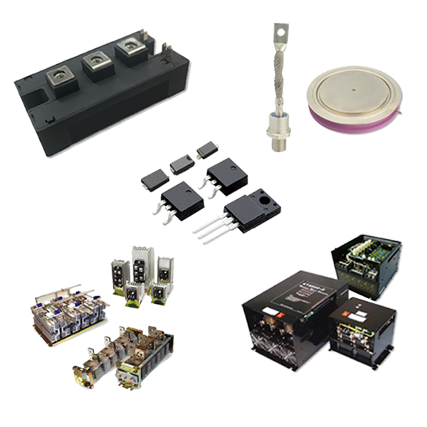
INDUSTRIES, APPLICATIONS & SYSTEMS USING SiC WAFERS


Power Electronics
SiC Schottky Diodes
SiC MOSFETs
SiC IGBTs
SiC Power Modules
SiC Converters & Inverters
SiC High-Power Rectifiers
SiC High-Voltage Switches & Power Supplies
Electric Vehicle (EV) Powertrains
Traction Inverters
On-Board Chargers (OBC)
EV Battery Chargers (DC Fast Chargers, Level 2 AC Chargers)
EV Thermal Management Systems
Aircraft Electrical Power Systems
Avionics Systems
Satellite Electronics
Spacecraft Power Management Units (PMU)
Satellite Communication Payloads

Industries
Electric Vehicles
Aerospace
Defense
Telecommunications
Data Centers
Sensors & High-Temperature Devices
SiC High-Temperature Sensors & Components
SiC Corrosion-Resistant Sensors/Devices
SiC Radiation-Resistant Sensors/Devices


Systems / Devices
Radar Systems (Ground-Based & Airborne)
Military Communication Systems
Missile Guidance & Control Systems
5G Base Stations
Wireless Communication Infrastructure
Data Centers (Power Supplies, Cooling Systems)
High-Performance Computing (HPC) Servers
Solar Inverters
Wind Turbine Converters
Renewable Energy
Grid Systems
Industrial & Automation
Medical
Research & Development

Applications
RF & Microwave Devices
SiC RF Transistors
SiC High-Frequency & Microwave Devices


Our SiC Wafers
4 inch Silicon Carbide Wafers 4H-SiC N-Type or Semi-Insulating SiC Substrates
4 inch High Purity (Undoped) Silicon Carbide Wafers Semi-Insulating SiC Substrates (HPSI)
6 inch Silicon Carbide Wafers 4H-SiC N-Type or Semi-Insulating SiC Substrates
6 inch High Purity (Undoped) Silicon Carbide Wafers Semi-Insulating SiC Substrates (HPSI)
8 inch Silicon Carbide Wafers 4H-SiC N-Type or Semi-Insulating SiC Substrates
8 inch High Purity (Undoped) Silicon Carbide Wafers Semi-Insulating SiC Substrates (HPSI)
Optoelectronics
SiC LEDs
SiC Optoelectronic Devices

Energy Storage Systems (ESS) Inverters
Grid-Tied Power Conversion Systems
Utility-Scale Power Distribution Systems
Smart Grid Infrastructure
High-Voltage Direct Current (HVDC) Transmission Systems
Motor Drives (Low & Medium Voltage)
Industrial Automation Equipment
Robotics Power Systems
Heavy-Duty Machinery (Construction, Agricultural, Mining)
Downhole Drilling Equipment

At Supreme Pro, we offer fully customizable SiC wafers and substrates to suit your unique needs, including specialized epitaxial options. Contact us today for a personalized quote and explore how our tailored solutions can elevate your projects.
Research Applications
SiC Quantum Computing Substrates
SiC Experimental/Prototype Devices
Offshore Oil & Gas Platform Power Systems
Chemical Reactor Power & Control Systems
Process Control Systems
Medical Imaging Equipment (MRI, CT, PET Scanners)
Radiation Therapy Machines
Portable Medical Devices (Diagnostic & Therapeutic)
University Laboratory Test Systems
Research Institution Prototypes
Technology Development & Pilot Centres