INDIUM PHOSPHIDE (InP) WAFERS
Powering High-Speed Connectivity
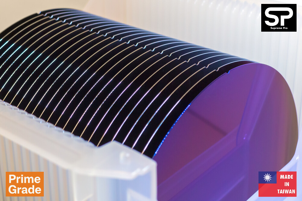
Image shown is a representation only. Exact specifications should be obtained from the product data sheet.Indium Phosphide (InP) wafers are critical for high-speed, high-frequency electronics and optoelectronics, driven by demand in 5G telecommunications, data centers, and LiDAR systems. Classified as a compound semiconductor, our InP wafers are the backbone of next-generation telecommunications and optoelectronic devices, enabling unmatched speed and efficiency. Engineered through our Singapore-Taiwan partnership, leveraging Taiwan’s 60% global semiconductor dominance, our MOCVD-grown InP wafers offer superior electron mobility, direct band gap, and thermal stability.
Designed for 5G networks, data centers, and LiDAR systems, they deliver low-noise, high-frequency performance for lasers, photodetectors, and photonic integrated circuits (PICs). With low-defect substrates and scalability to 6-inch wafers, our InP wafers accelerate your innovations in high-speed, high-efficiency applications.
Our InP Wafers
2 Inch Semi-Insulating Fe-Doped InP Epitaxial Wafer
2 Inch N-Type Sulfur-Doped InP Template Wafer
3 Inch Semi-Insulating Undoped InP Epitaxial Wafer
3 Inch P-Type Zinc-Doped InP Epitaxial Wafer
4 Inch Semi-Insulating Undoped InP Epitaxial Wafer
4 Inch N-Type Sulfur-Doped InP Template Wafer
6 Inch Semi-Insulating Fe-Doped InP Epitaxial Wafer
6 Inch N-Type Sulfur-Doped InP Wafer for Photovoltaics
+ We offer fully customizable InP wafers and substrates to suit your unique needs, including specialized epitaxial options. Contact us today for a personalized quote and explore how our tailored solutions can elevate your projects.
WHY CHOOSE InP WAFERS?
Superior Speed
High electron mobility (5,400 cm²/V·s) enables 300 GHz operation, critical for 5G and data center markets.
Optoelectronic Efficiency
Direct bandgap (1.35 eV) delivers 35%+ efficiency in lasers and solar cells, outperforming silicon .
Reliability
Low EPD (≤500/cm²) and radiation resistance ensure consistent performance in harsh environments.
Compact Solutions
30% smaller RF and photonic components meet demand for miniaturized 5G and LiDAR devices.
Future-Proof
Aligned with the $586.75 million InP market’s 13.77% CAGR, our wafers drive innovation in telecom and automotive.
WHY CHOOSE US?
Our InP Wafers lead in a competitive market, powered by Singapore’s market agility and Taiwan’s world-class semiconductor expertise. Here’s why global buyers trust us:


Uncompromising Quality
Partnering with Taiwanese leaders, we deliver MOCVD-grown InP wafers with EPD ≤500/cm², meeting JEDEC and MIL-STD standards for telecom and aerospace applications.
Cost Optimization
Our 6-inch wafers and optimized epitaxy reduce costs by up to 20%, addressing buyer concerns about InP’s high cost vs. silicon.
Custom Solutions
Tailored doping (S, Zn, semi-insulating) and wafer sizes meet specific project needs, mirroring AXT’s application-specific approach.
Sustainability Focus
High-efficiency InP devices reduce energy use by 25%, supporting green initiatives in 5G and data centers.


Advanced Manufacturing
Using MOCVD and MBE processes in Taiwan’s cleanrooms, we achieve high-uniformity 6-inch wafers, matching Coherent Corp.’s industry-first 6-inch InP production for cost efficiency.
Reliable Supply Chain
Unlike competitors facing indium supply constraints (80% from China), our Singapore-Taiwan synergy ensures stable supply, inspired by Sumitomo Electric’s global sourcing strategy.
Global Trust
Certified to ISO 9001, ISO 14001, RoHS, and REACH, our wafers are trusted by OEMs in 50+ countries, backed by Taiwan’s 90% advanced chip share.
Contact Us: Ready to elevate your designs with our InP Wafers? Click below to request a quote or discuss custom specifications.
SPECIFICATIONS
Material: InP (III-V compound semiconductor, zinc blende structure)
Diameter: 2-inch (50mm), 4-inch (100mm), 6-inch (150mm) (scalable for high-volume production)
Thickness: 350–625 µm (customizable per application)
Etch Pit Density (EPD): ≤500/cm² (low-defect for high reliability)
Surface Finish: Metal Organic Chemical Vapor Deposition (MOCVD) or Molecular Beam Epitaxy (MBE), mirror-like, Ra <0.3 nm
Doping: N-type (S-doped, >1000 cm²/V·s), P-type (Zn-doped, 80±10 cm²/V·s), Semi-Insulating (>2000 cm²/V·s)
Electron Mobility: 5,000–5,400 cm²/V·s (4x silicon for high-speed performance)
Band Gap: 1.35 eV (direct, enabling efficient light emission/absorption)
Thermal Conductivity: 68 W/m·K (optimized for high-frequency devices)
Breakdown Electric Field: 0.5 MV/cm (supports high-voltage RF applications)
Crystal Orientation: (100), optimized for HEMTs, HBTs, and PICs
Packaging: Class 100 cleanroom, vacuum-sealed for contamination-free delivery
Contact Us: Inquire about custom specifications or pricing. Click below to connect with our team.
STANDOUT FEATURES


Direct Band Gap
1.35 eV supports efficient light emission/absorption, perfect for lasers, photodetectors, and PICs.
High-Frequency Performance
Up to 300 GHz operation with low noise, enabling 5G base stations and satellite communications.
Radiation Resistance
Resists radiation damage 10x better than silicon, ensuring reliability in space and military applications.

High Electron Mobility
5,000–5,400 cm²/V·s enables ultra-fast switching, ideal for 5G RF amplifiers and high-speed ICs.
Thermal Stability
68 W/m·K and robust crystal structure ensure performance in high-power, high-frequency devices.
Low Defect Density
EPD ≤500/cm² ensures high reliability and yield for telecommunications and aerospace applications.
ADDITIONAL BENEFITS

Energy Efficiency
25% lower power consumption than silicon, reducing operating costs in data centers and consumer devices.

Reliability
Radiation resistance and thermal stability ensure longevity in aerospace and defense systems.
Compact Designs
High electron mobility allows 30% smaller RF and photonic components, ideal for 5G smartphones and LiDAR.

Lower Noise
Reduced signal distortion in high-frequency circuits, enhancing performance in optical communications.
Contact Us: Discover how our InP Wafers can optimize your designs. Click below for a quote.
High Conversion Capability
InP solar cells achieve 35%+ efficiency, outperforming silicon for space applications.

Scalable Wafer Sizes
2-inch to 6-inch diameters, with 6-inch offering 2x more chips per wafer, reducing costs.
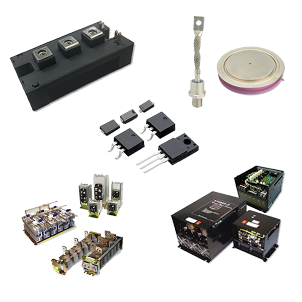
INDUSTRIES, APPLICATIONS & SYSTEMS USING InP WAFERS


High-Speed Electronics
InP High-Speed Transistors (HBTs, HEMTs)
InP High-Frequency Amplifiers / Circuits
InP High-Speed Switches
InP High-Frequency Receivers
Fiber-optic communication networks (metro, access, backbone)
Data center interconnects & optical links
Long-haul communication systems (submarine, transcontinental)
5G wireless backhaul & fronthaul infrastructure
Optical transceivers for high-speed internet (400G/800G)
Free-space optical communication systems
Smartphones & wearables (VCSELs, photodetectors for facial recognition, LiDAR)
Augmented reality (AR) & virtual reality (VR) devices (optical sensing & projection)
High-speed data processors with integrated photonics
InP-based LiDAR systems for autonomous driving (Tesla, BMW, Audi, etc.)
Automotive radar for ADAS (advanced driver-assistance systems)
In-vehicle optical communication networks (future automotive photonics)
Satellite communication payloads (transponders, laser crosslinks)

Industries
Telecommunications
Data Centers
Consumer Electronics
Electric Vehicles
Aerospace
RF, Terahertz & Imaging
InP Terahertz Devices / Test Devices
InP Terahertz Imaging & Waveguide Devices

Systems / Devices
Defense
Renewable Energy
Medical
Industrial & Scientific Applications
Research & Advanced Technology

Applications
Our InP Wafers
2 Inch Semi-Insulating Fe-Doped InP Epitaxial Wafer
2 Inch N-Type Sulfur-Doped InP Template
3 Inch Undoped Semi-Insulating InP Epitaxial Layer
3 Inch P-Type Zinc-Doped InP Wafer
4 Inch Semi-Insulating Undoped InP Epitaxial Wafer
4 Inch N-Type Sulfur-Doped InP Template
6 Inch Semi-Insulating Fe-Doped InP Epitaxial Structure
6 Inch N-Type Sulfur-Doped InP Wafer for Photovoltaics
Photonics & Optoelectronics
InP Laser Diodes / Laser Sources
InP Quantum Cascade Lasers (QCLs)
InP Photodetectors / High-Speed Photodiodes
InP Optical Sensors / Photonic Sensors
InP Modulators
InP Photonic Integrated Circuits (PICs) / Integrated Optical Circuits
InP Photonic Components / Emitters
InP Optical Communication Modules


Research & Emerging Technologies
InP Quantum Dot Structures / Substrates
InP Experimental Photonic Chips / Substrates

Spaceborne sensors (remote sensing, hyperspectral imaging)
Space navigation & tracking systems
Deep-space probes (laser-based interplanetary communication)
Space exploration electronics (radiation-hardened optoelectronics)
Space solar arrays & concentrated photovoltaic (CPV) cells
Radar systems (ground, airborne, naval)
Sonar & undersea communication systems
Missile guidance & targeting technology
Secure military optical communication networks
Tactical battlefield communication systems
Security scanners & surveillance equipment
Thermal imaging cameras & night-vision optics
High-efficiency multi-junction solar cells (InP + GaAs + Ge stacks)
Space solar panels for satellites & spacecraft
Concentrated solar power (CSP) systems with InP-based cells

At Supreme Pro, we offer fully customizable InP wafers and substrates to suit your unique needs, including specialized epitaxial options. Contact us today for a personalized quote and explore how our tailored solutions can elevate your projects.
Energy & Space Applications
InP High-Efficiency Solar Cells
InP Multi-Junction Solar Cells
InP High-Efficiency Photovoltaic Devices
InP Radiation-Hardened / Radiation-Tolerant Devices
Laser surgery systems (ophthalmology, oncology, dermatology)
Ophthalmic surgery tools (e.g., LASIK systems)
Endoscopy & minimally invasive surgical tools
Diagnostic imaging systems (optical coherence tomography, spectroscopy)
Radiation therapy imaging & monitoring systems
Precision manufacturing lasers (micro-machining, lithography alignment)
Automated control & monitoring systems
Spectroscopy equipment (chemical & material analysis)
Security & industrial scanners (airports, border control)
Quantum computing labs (InP-based photonic qubits, quantum communication)
Material science & photonics research
University & academic research labs
Innovation labs & prototyping centers
Technology development programs (defense, telecom, healthcare R&D)