
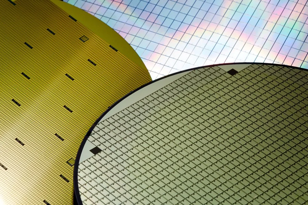
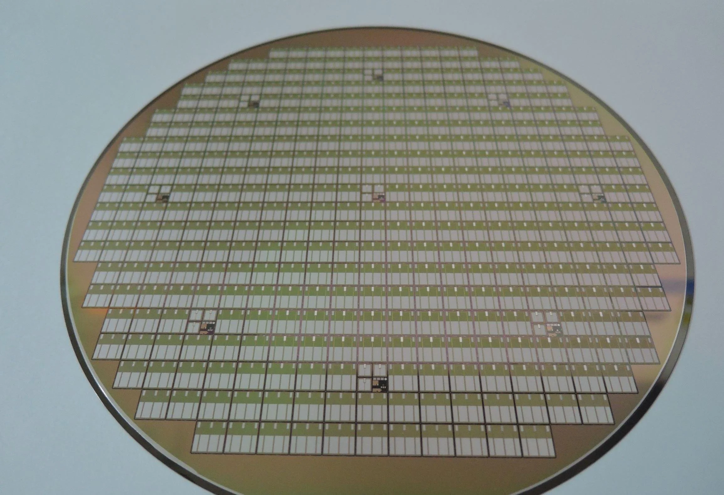
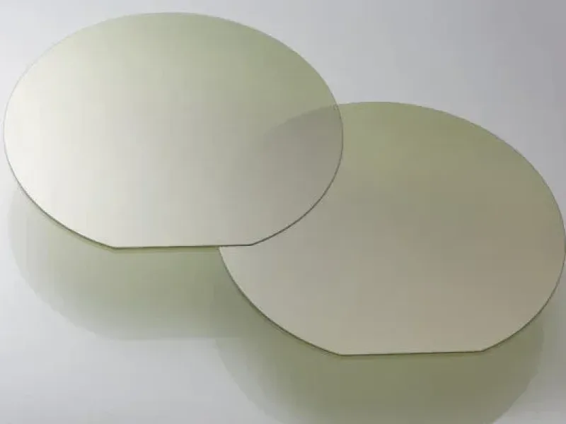
Silicon Carbide (SiC) Wafers
At Supreme Pro, we take pride in offering an exceptional range of high-quality SiC Wafers, available in diameters up to eight inches, featuring N-type, P-type, and semi-insulating variants. Trusted globally by leading semiconductor firms and cutting-edge research institutions, our SiC solutions are engineered to meet the rigorous demands of modern technology.

+ We offer fully customizable GaN wafers and substrates to suit your unique needs, including specialized epitaxial options. Contact us today for a personalized quote and explore how our tailored solutions can elevate your projects.

Our SiC Wafers


Why Choose SiC Wafers?
SiC wafers are premium materials designed for the semiconductor industry, composed of a robust silicon-carbide compound. Renowned for their outstanding thermal conductivity, superior mechanical durability, and wide band gap, these substrates provide a solid base for developing advanced high-power and high-frequency electronic components, including power management systems and radio frequency devices. With their remarkable hardness and lightweight nature, SiC wafers excel in challenging conditions, offering a dependable platform for cutting-edge innovations.
The distinctive attributes of SiC wafers make them the go-to choice for applications demanding high-temperature resilience, operation in extreme environments, and enhanced energy efficiency, setting them apart in the semiconductor landscape.
Advantages Over Traditional Silicon
Compared to conventional silicon-based devices, Silicon Carbide wafers empower the creation of power devices with rapid switching capabilities, support for higher voltages, reduced parasitic resistances, more compact designs, and minimized cooling needs thanks to their exceptional high-temperature performance.


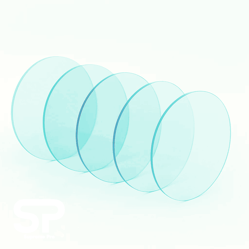
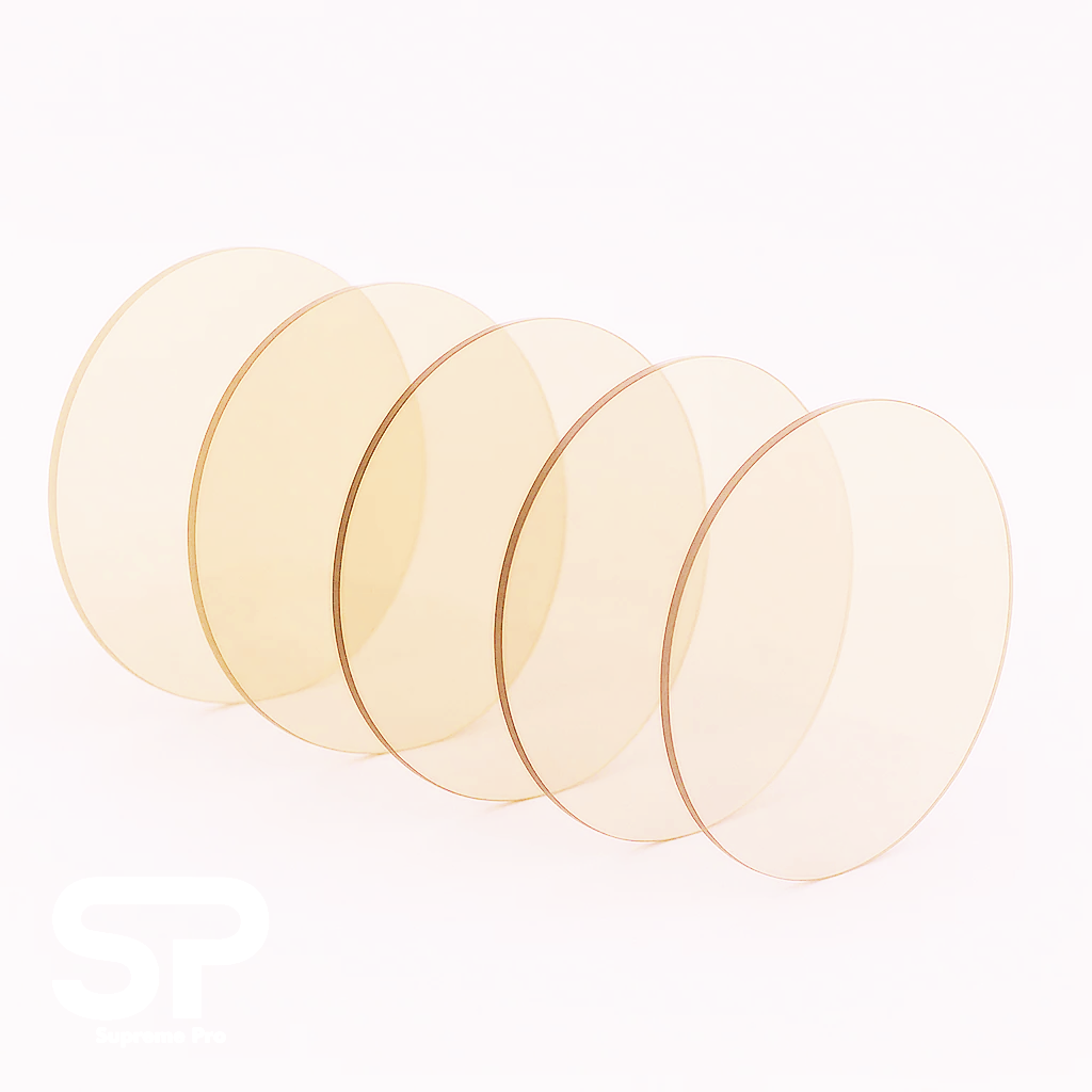
Image shown is a representation only. Exact specifications should be obtained from the product data sheet.

Applications of SiC Wafers
Supreme Pro’s SiC wafers are the backbone of a wide array of electronic solutions, including power diodes, MOSFETs, high-power microwave devices, and RF transistors, optimizing energy conversion and power control. These wafers also play a vital role in automotive electronics, aerospace technologies, and renewable energy systems, pushing the boundaries of performance.
Additionally, our SiC substrates are integral to gas and chemical sensors, as well as pioneering research areas such as quantum computing and high-frequency communications, fueling breakthroughs across diverse technological fields. They serve as an excellent foundation for epitaxial growth of GaN and high-power MMIC devices, enhancing their versatility.
Specifications
Material: 4H-SiC (primary polytype for power electronics; 6H-SiC for specific RF applications)
Diameter: 100mm, 150mm, 200mm (8-inch gaining traction for high-volume cost efficiency)
Thickness: 350–500 µm (customizable, with ±25 µm tolerance for standard grades)
Micropipe Density (MPD): ≤1/cm² (Ultra-Prime Grade) or ≤5/cm² (Prime Grade) for low-defect performance
Resistivity Uniformity: ≥95% (ensuring consistent doping across the wafer)
Surface Finish: Chemical Mechanical Polishing (CMP), epi-ready, Ra <0.2 nm for optimal epitaxial growth
Doping: N-type (nitrogen-doped, resistivity 0.015–0.028 Ω·cm) or semi-insulating (vanadium-doped, >10^5 Ω·cm)
Thermal Conductivity: 370–490 W/m·K (superior heat dissipation, 3x silicon)
Breakdown Electric Field: 2.5–3.5 MV/cm (10x silicon for high-voltage resilience)
Bandgap: 3.26 eV (wide bandgap enabling 3x silicon's temperature tolerance)
Crystal Orientation: (0001) with 4° off-axis (optimized for epitaxial layer quality in power devices)
Total Thickness Variation (TTV): <5 µm (for uniform processing)
Bow/Warp: <25 µm bow, <40 µm warp (minimizing handling issues)
Packaging: Class 100 cleanroom, vacuum-sealed in anti-static containers for contamination-free transport
Selecting the Right SiC Wafers
Choosing the ideal SiC wafer from Supreme Pro involves careful consideration of several key factors:
Doping Type: Opt for N-type (e.g., nitrogen-doped) or semi-insulating (e.g., vanadium-doped) variants to align with power device requirements or high-frequency applications.
Wafer Diameter: Select sizes from 2" to 8", with 6" and 8" becoming standard for scaling production, ensuring compatibility with advanced fabrication tools.
Surface Finish: Prioritize epi-ready surfaces with roughness below 0.2 nm RMS to support high-quality epitaxial growth for MOSFETs and diodes.
Crystal Polytype: Choose between 4H-SiC or 6H-SiC based on application needs, with 4H preferred for power electronics due to higher electron mobility.
Micropipe Density (MPD): Target MPD below 5 cm⁻² to minimize defects that impact device reliability in high-voltage environments.
Resistivity: Select semi-insulating (10⁶–10⁹ Ω·cm) for RF applications or conductive (0.015–0.028 Ω·cm) for power devices to match electrical performance.
Thickness Uniformity: Ensure thickness variation less than 5 μm across the wafer to maintain consistent thermal and electrical properties during processing.
Bow and Warp: Aim for bow and warp values below 15 μm and 30 μm respectively to prevent issues in photolithography and device stacking.
At Supreme Pro, we offer fully customizable SiC wafers and substrates to suit your unique needs, including specialized epitaxial options. Contact us today for a personalized quote and explore how our tailored solutions can elevate your projects.

Our SiC Wafers
4 in Silicon Carbide Wafers 4H-SiC N-Type or Semi-Insulating SiC Substrates
4 inch High Purity (Undoped) Silicon Carbide Wafers Semi-Insulating SiC Substrates (HPSI)
6 in Silicon Carbide Wafers 4H-SiC N-Type or Semi-Insulating SiC Substrates
6 inch High Purity (Undoped) Silicon Carbide Wafers Semi-Insulating SiC Substrates (HPSI)
8 in Silicon Carbide Wafers 4H-SiC N-Type or Semi-Insulating SiC Substrates
8 inch High Purity (Undoped) Silicon Carbide Wafers Semi-Insulating SiC Substrates (HPSI)